01 / System boundary
A package is no longer a protective shell
Modern AI silicon is assembled as a local system before it ever reaches a server board.
Traditional descriptions place packaging after fabrication, as though the difficult work ends when a good die leaves the wafer. AI accelerators overturn that sequence. Logic dies, memory stacks, passive structures, power-delivery paths, and high-density links must be integrated at distances short enough to move enormous volumes of data without the energy and latency penalties of a conventional board trace.
That makes the package an architectural boundary. Decisions about die partitioning, memory placement, interposer size, substrate routing, bump pitch, and heat removal constrain the accelerator long before a rack designer chooses a chassis. A brilliant die that cannot be assembled, powered, cooled, tested, or produced at acceptable yield is not deployable compute; it is unfinished inventory.
Read the stack
- Die
- A tested piece of patterned semiconductor cut from a wafer.
- Package
- The electrical, mechanical, and thermal assembly that makes one or more dies usable by a system.
- Module
- A packaged device plus the board, connectors, and local components needed for integration.
Three envelopes must agree
- Design envelope
- Die area, edge length, routing demand, power delivery, thermal paths, and protocol boundaries that the architecture requires.
- Manufacturing envelope
- Available substrate formats, alignment capability, material controls, inspection coverage, qualified tools, and recoverable yield at each assembly stage.
- Operating envelope
- Temperatures, currents, workload duty cycles, repair policies, and error rates within which the completed package must remain dependable.
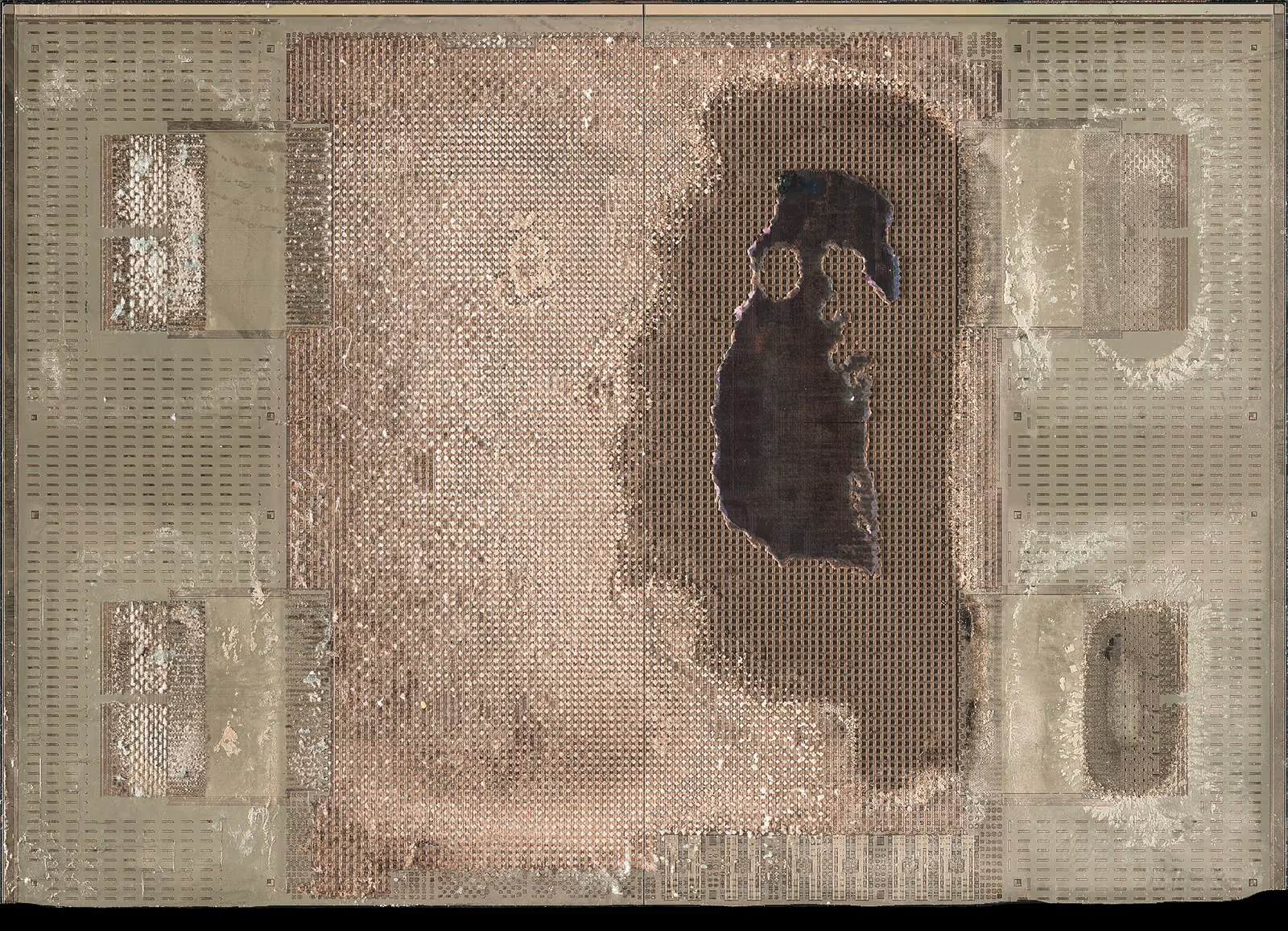
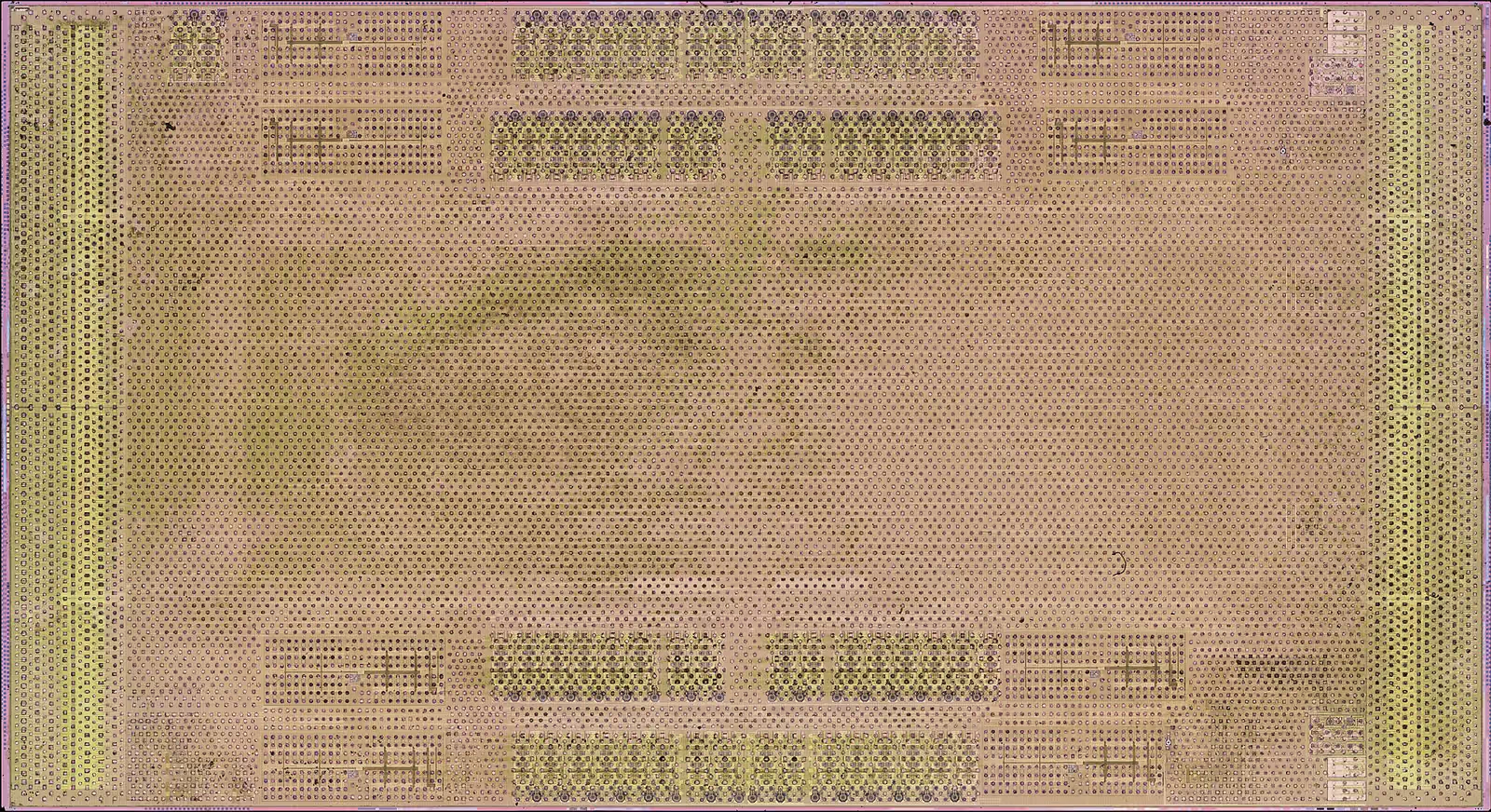
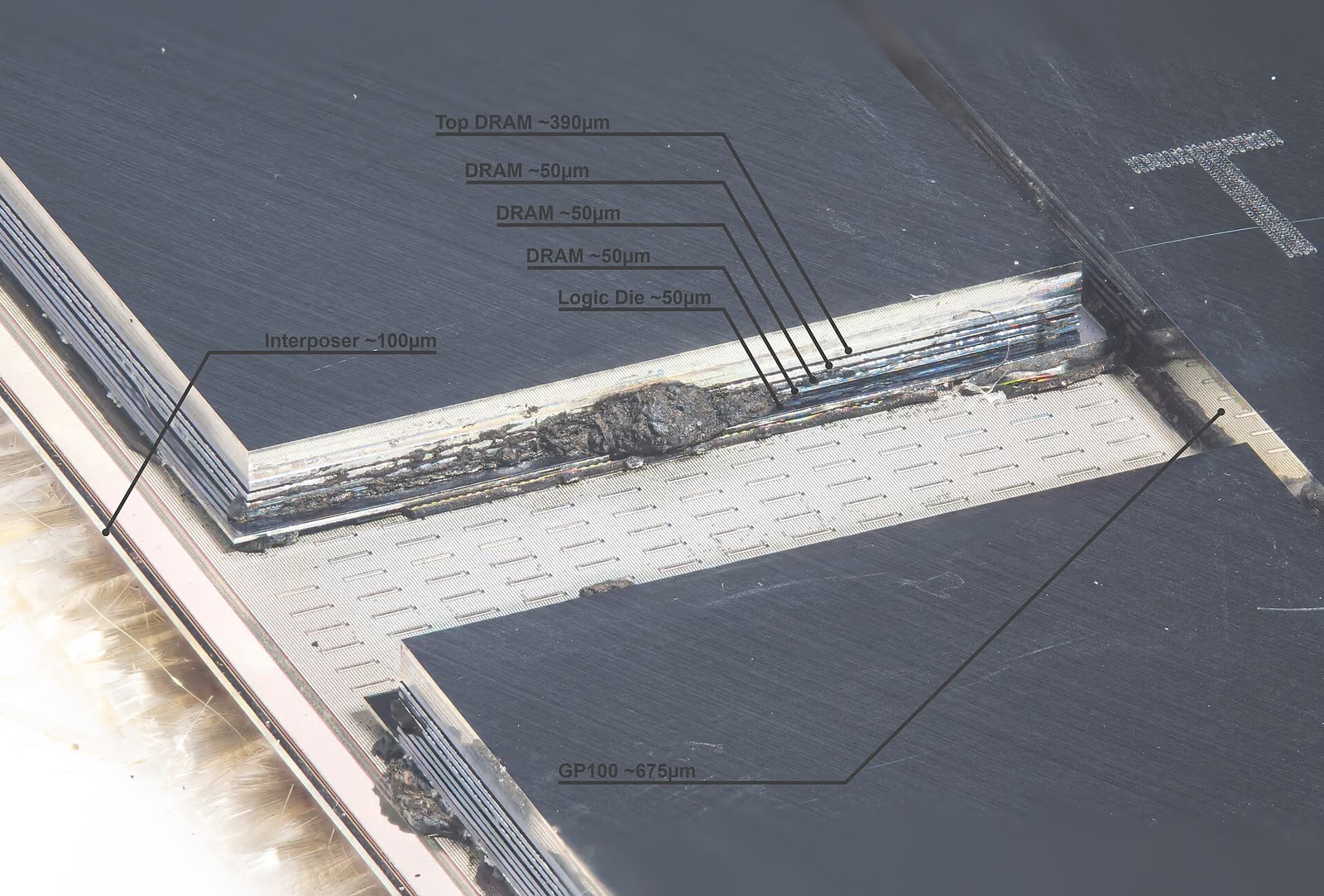
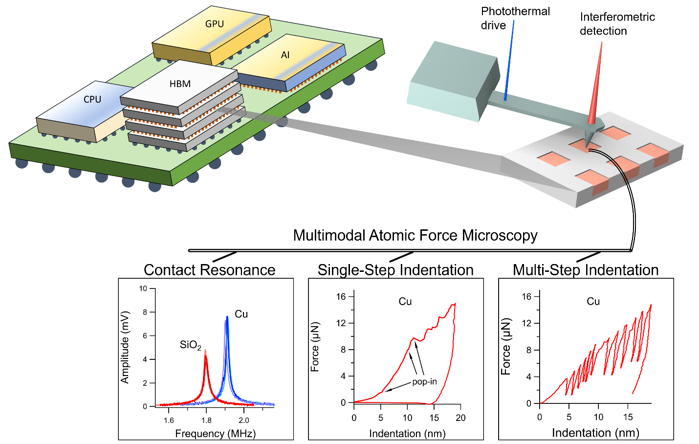

@Zen2@Rome@EPYC_7702_ES@2S1404E2VJUG5_BB_ES_DSCx6_IOD_top_metal@5x.jpg)
