Intelligence BuildoutMethodology

Precision — complete text edition

Volume II / Text edition

Precision

Chip design + wafer fabrication. 15 spreads and 30 pages, with the complete evidence-linked content. No JavaScript is required.

Volume II

Precision

Chip design + wafer fabrication · 30 pages

See how workload intent becomes verified geometry, how lithography and process tools reproduce it on silicon, and why yield—not installed machinery—defines productive capacity.

01

From workload to tape-out

Architecture, IP, tools, process rules, software, and verification converge before a mask set can direct a single exposure.

Spread 01 / Workload becomes architecture

Volume II · Orientation

A chip begins as a decision system

Architecture is the negotiated answer to what work matters, what must move, and which constraints cannot be escaped.

AI workloads combine dense arithmetic, memory access, synchronization, communication, control, and storage. Training and inference weight these behaviors differently, while model shape, numerical format, batch size, latency target, reliability, and software ecosystem change the balance again. Hardware teams translate that workload envelope into throughput, memory, interconnect, power, area, and programmability targets.

PyTorch documents data, sharded-data, tensor, and pipeline parallelism as complementary distributed-training approaches. Those software choices are also hardware questions: they influence local memory capacity, accelerator-to-accelerator links, collective operations, host coordination, and how failure or stragglers affect the whole job.Claim

Design boundary: There is no universally best accelerator. A design is good only relative to workloads, deployment constraints, software readiness, cost, and time.
Turn a workload claim into a design contract
  1. Characterize— Describe operation mix, tensor shapes, precision, sparsity, locality, sequence behavior, and synchronization.
  2. Constrain— Set latency, throughput, power, thermal, memory, reliability, security, and cost boundaries.
  3. Model— Estimate compute, movement, storage, communication, and control bottlenecks across representative cases.
  4. Prototype— Compare architecture choices with traceable assumptions and sensitivity tests.
  5. Freeze— Record the benchmark, software stack, corner cases, and acceptance rule that authorize implementation.
Value chain

The first factory is informational

Before silicon processing, teams manufacture confidence through models, specifications, simulations, and reviews.

SIA's semiconductor value-chain overview places research and design before front-end fabrication, assembly, test, and product integration. That order matters because design data becomes the instruction set for expensive physical operations. An architectural mistake discovered after tape-out can consume masks, wafer starts, packaging capacity, engineering time, and market schedule.Claim

Early design therefore works through nested abstractions. Workload models inform architecture; architecture becomes functional blocks and interfaces; logic becomes timed circuits; circuits become geometry matched to foundry rules. At each stage, teams ask whether the representation still satisfies function, power, performance, area, testability, manufacturability, and software assumptions.

Intent path
  1. Observe— Characterize workloads and deployment limits.
  2. Architect— Partition compute, memory, control, and movement.
  3. Implement— Convert functions into timed, manufacturable geometry.
  4. Verify— Challenge behavior, interfaces, and physical rules.
  5. Release— Freeze pattern data for mask generation.
Workload evidence changes different hardware decisions
ObservationLikely pressureAudit question
Low reuseMemory bandwidth and data movementWas locality measured on production-like inputs?
Irregular controlScheduling and general-purpose executionWhich divergence and tail cases dominate?
Collective trafficFabric topology and synchronizationDoes the model include congestion and stragglers?
Strict latencyQueueing, memory, and software overheadIs the percentile and load level explicit?

Spread 02 / Compute architectures

Architecture

GPU, CPU, ASIC, and DPU divide the work

A useful AI system assigns different tasks to engines optimized for different forms of parallelism and control.

Accelerators devote substantial area and power to parallel arithmetic, local memory movement, and high-throughput data paths. CPUs remain important for orchestration, serial work, operating systems, and application logic. Purpose-built ASICs can narrow the workload contract further, trading generality for efficiency. DPUs and related infrastructure processors move networking, security, storage, or virtualization duties away from hosts.

These labels describe roles, not fixed internal designs. A modern device may mix matrix engines, vector units, scalar cores, caches, controllers, packet processing, compression, and security blocks. System performance depends on the balance: unused arithmetic is not useful if memory, interconnect, software, or scheduling cannot feed it.

Architectural role and primary tension
RoleOptimizes forCommon tension
AcceleratorParallel throughput and data reuseProgrammability and utilization
CPUControl, compatibility, and varied tasksThroughput per watt for dense kernels
ASICA bounded workload contractFlexibility as models change
DPUInfrastructure and data movementSystem integration complexity
Architecture is a bottleneck allocation
Throughput regime
Many units of work can be batched; utilization and aggregate work per time dominate.
Latency regime
A response deadline limits batching and exposes queue, memory, and communication delay.
Bandwidth regime
Data delivery constrains useful operations even when arithmetic units remain available.
Capacity regime
Working-set size or state placement determines whether the workload fits efficiently.
Control regime
Branching, orchestration, and irregular work favor flexibility over dense specialization.

Interfaces

An instruction set is a durable agreement

The visible software contract and the hidden microarchitecture solve different parts of the problem.

The RISC-V architecture is organized around a required base instruction set plus optional standardized extensions. That modular structure illustrates a broader design principle: stable interfaces let software and hardware evolve with some independence, while optional features allow implementations to target different products.Claim

Below the instruction set, microarchitecture decides pipelines, execution units, queues, prediction, caches, clocking, and data movement. Around it, coherent links, memory controllers, security roots, test logic, and physical interfaces connect the die to a package and system. Each block brings verification work and constrains floorplan, power distribution, thermal density, and manufacturability.

Layers of the contract
ISA
The programmer-visible instruction and state model.
Microarchitecture
One internal implementation of that visible contract.
IP block
A reusable design component with defined interfaces and evidence.
System architecture
How devices, memory, links, power, and software work together.
Audit the software boundary with the silicon
  • Identify which instructions, data types, kernels, libraries, compilers, and communication primitives are production dependencies.
  • Separate theoretical peak from achieved performance after layout, memory stalls, synchronization, and software overhead.
  • Test portability claims with the actual model graph, numerical tolerances, observability, and failure recovery.
  • Record which features are fixed in hardware, updateable in firmware, generated by a compiler, or scheduled at runtime.
  • Price migration in engineering time and correctness risk, not only in replacement hardware.

Spread 03 / Chiplets, IP, and process rules

Partition

Chiplets move the boundary, not the difficulty

Splitting a system across dies can improve reuse and manufacturing choices while adding interfaces, packaging, and verification obligations.

A monolithic die keeps many functions on one piece of silicon. A chiplet strategy partitions compute, input/output, cache, analog, or other functions across dies that may use different processes. The approach can support modular products and avoid placing every function on the most demanding process, but the package now carries system-level connectivity.

Partitioning decisions must account for die area, expected yield, link bandwidth, latency, energy per bit, clocking, power delivery, thermal coupling, test coverage, and known-good-die supply. An elegant block diagram can fail commercially if package capacity, interface validation, or assembly yield cannot support the resulting product.

AI relevance: Chiplets can place more compute and memory-side capability in one system envelope, but they make package architecture a first-order design discipline.
Partitioning moves constraints to the die boundary
BoundaryDesign questionFailure mode
DataWhat bandwidth, latency, protocol, and ordering are required?Congestion or serialization loss
Clock and resetHow do domains start, cross, recover, and diagnose?Intermittent or unrecoverable state
Power and thermalWhere are delivery limits and coupled hot spots?Droop, throttling, or accelerated aging
Test and repairCan each die and link be screened, isolated, and traced?Known-bad assembly or poor diagnosis

Foundry interface

The PDK turns a factory into design rules

Designers do not draw abstract transistors; they implement within a documented, versioned manufacturing capability.

A process design kit packages models, layer definitions, layout rules, device options, extraction data, and verification checks for a foundry process. Standard-cell and interface libraries add characterized building blocks. EDA tools use those artifacts to estimate timing, power, noise, density, and manufacturability before physical release.

The global semiconductor chain distributes design, EDA, IP, materials, equipment, fabrication, and assembly across specialized clusters. A PDK and its approved tool flow are where several of those clusters meet. Version changes, library availability, export rules, or capacity choices can alter the design path long before any wafer moves.Claim

PDK questions
  • Which device and interconnect options are supported?
  • Which verification decks and tool versions are qualified?
  • What reliability, voltage, and temperature limits apply?
  • Which IP has been characterized for the target process?
  • What changes require design re-signoff?
A PDK is an executable manufacturing agreement
  1. Model— Represent device, interconnect, variation, reliability, and extraction behavior within stated corners.
  2. Constrain— Encode legal geometry, density, antenna, power, and integration rules.
  3. Build— Provide cells, memories, interfaces, and reference flows with traceable versions.
  4. Verify— Check logical, electrical, timing, and physical consistency against the selected release.
  5. Control— Assess every PDK update for affected blocks, signoff reruns, waivers, and tape-out compatibility.
A tape-out is tied to a particular process, rule set, and evidence package.

Spread 04 / Verification and tape-out

Verification

Confidence is built from different kinds of proof

No single simulation can establish that a complex device is functionally correct, physically legal, manufacturable, and useful in software.

Functional verification challenges logic with directed tests, constrained random stimulus, assertions, formal methods, emulation, and workload traces. Physical signoff checks timing, power integrity, layout rules, connectivity, signal integrity, reliability limits, and manufacturability. Design-for-test adds structures that make finished devices observable and screenable.

Verification is risk prioritization under finite schedule. Teams track coverage, unresolved assumptions, waivers, model correlation, and change impact. The hardest defects often sit at interfaces: clock and reset sequences, memory ordering, coherency, low-power states, error recovery, chiplet links, and firmware interactions. Evidence must follow those interfaces across organizational boundaries.

NIST's advanced-packaging program identified roughly one hundred million design instances as the point above which contemporary EDA abstractions made full-chip implementation impractical and forced partitioning into blocks. The figure is an approximate program assessment, not a universal tool ceiling; its operational meaning is that partition interfaces, package behavior, and cross-block verification become first-class schedule risks.Claim

The cost boundary is similarly large but must stay dated. A 2021 U.S. supply-chain review reproduced industry estimates of 297.8 million dollars for a 7 nm design and 542.2 million dollars for a 5 nm design; NIST's current program says functional verification accounts for more than half of new-chip design cost. The first figures are 2018–2019 estimates, not 2026 budgets, while the second is a program premise rather than an audited market census.ClaimClaim

Signoff ladder
  1. Function— Does the logic satisfy its specified behavior?
  2. Timing— Can data arrive correctly across operating conditions?
  3. Power— Can the network deliver current without unsafe noise or heat?
  4. Geometry— Does layout follow foundry and connectivity rules?
  5. Test— Can production detect defects and isolate failure?
Closure is evidence against different bug classes
EvidenceQuestion answeredResidual risk
SimulationDid exercised scenarios behave as expected?Unexercised state and unrealistic environment
Formal analysisDoes a bounded property hold over modeled states?Incorrect properties or abstraction
Emulation/prototypeDoes integrated hardware-software behavior run at useful scale?Model and implementation differences
Static signoffDo timing, power, electrical, and physical rules close at stated corners?Missing corners, models, or exceptions

Release

Tape-out freezes a physical hypothesis

Release sends verified geometry toward mask creation, while software and system work continue against the expected device.

At tape-out, the implementation is checked, versioned, approved, and converted into the data used to manufacture masks. The term suggests a moment, but the release is a controlled evidence package: design databases, rule results, waivers, revision history, test intent, and ownership of remaining risk.

CUDA and ROCm each span programming models, runtimes, compilers, libraries, debugging tools, and hardware interfaces. That stack cannot be bolted on after fabrication. Compiler behavior, numerical support, memory semantics, profiling, firmware, and libraries feed hardware choices and provide pre-silicon workloads for verification.Claim

NIST's current SoC architecture program explicitly joins hardware/software co-design with heterogeneous packaged components. That makes the field-guide sequence circular rather than linear: workload and software constrain architecture; architecture and package constrain verification; pre-silicon evidence then returns to compiler, firmware, and runtime work before tape-out.Claim

Tool access is also an industrial dependency. CRS attributed seventy-two percent of worldwide EDA and semiconductor-IP revenue in 2021 to U.S.-headquartered firms, while the FTC's 2025 Synopsys–Ansys order required divestitures in three defined software-tool markets. Neither record proves one current market share across all EDA, but together they show why licenses, qualified flows, foundry relationships, and continuity plans belong in tape-out diligence.ClaimClaim

Cost of ambiguity: A late misunderstanding can propagate from architecture into masks, wafers, packages, boards, and software. Configuration control is part of manufacturing precision.
Tape-out change discipline
  1. Baseline— Freeze design, constraints, libraries, PDK, tools, waivers, and signoff reports under one identity.
  2. Classify— Determine whether a late change affects function, timing, power, physical rules, test, mask data, or documentation.
  3. Bound— Prove which hierarchy, corners, and downstream artifacts are touched rather than assuming locality.
  4. Rerun— Execute the complete affected verification set and compare against the accepted baseline.
  5. Authorize— Require accountable approval and preserve the exact released database and evidence package.
02

Masks, light, and projection

Lithography transfers design geometry into photoresist, but its useful result depends on mask making, optics, mechanics, chemistry, computation, and control.

Spread 05 / Masks and pattern data

Reticle data

The mask is manufactured information

Layout geometry is transformed, written, inspected, repaired where possible, and qualified before it can guide wafer exposure.

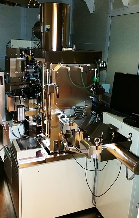
Tall direct-write electron-beam lithography tool installed inside a cleanroom.

Electron-beam equipment provides a documentary view of the precision tooling used to write or inspect nanoscale patterns.

The image is illustrative of electron-beam work; it does not depict a complete commercial EUV mask-production line or a specific AI chip mask set.The NIST item carries no copyright mark. Identification of visible equipment does not imply NIST endorsement.Credit: NIST.Original sourceNIST public information

A mask set begins with fractured pattern data derived from the signed-off layout. Writing tools form the pattern on a prepared blank; metrology and inspection compare the result with intent. Defects may be repaired or force a rewrite. Data handling, write time, pattern complexity, blank quality, and inspection sensitivity all influence schedule.

The mask is not a simple photographic negative. Optical and process corrections can make its shapes differ from the features intended on silicon. The pattern is engineered so that source, optics, resist, etch, and process conditions together produce the desired wafer geometry.

Mask-data release controls
  • Verify hierarchy, layer mapping, polarity, tone, bias, optical corrections, and fracture settings against the intended process.
  • Preserve checksums and lineage from signed layout through transformed mask-write data and delivered plate.
  • Inspect critical and repeating defects according to how they print, not only how they appear on the plate.
  • Control pellicle, cleaning, handling, storage, transport, and tool history as part of the qualified mask state.
  • Link every repair, waiver, and requalification to affected layers, fields, products, and exposure conditions.

Protection and control

A small defect can repeat across many fields

Because a reticle is reused, contamination and pattern errors can become systematic rather than isolated.

Reticle handling controls particles, electrostatic events, mechanical damage, contamination, and identity. A pellicle, where used, holds particles away from the pattern plane so they are less likely to print, but it introduces its own transmission, thermal, mechanical, and inspection considerations. Mask lifecycle includes storage, cleaning, inspection, exposure history, and version control.

EUV uses 13.5-nanometer light, which changes mask and optical behavior relative to transmissive DUV systems. The engineering response includes reflective masks and a mirror-based path. The wavelength does not directly equal printed feature size; imaging, numerical aperture, resist, process correction, and pattern strategy all contribute.Claim

Mask control record
  • Design and correction-data revision
  • Blank, write, inspection, and repair history
  • Defect disposition and accepted waivers
  • Pellicle and cleaning status
  • Exposure count and retirement criteria
A mask has both a defect and a lifecycle state
StateRelease evidenceStop condition
WrittenData identity and write completionMismatch, write interruption, or unreviewed deviation
InspectedDefect map tied to printability criteriaCritical or repeating defect above disposition rule
RepairedPost-repair inspection and affected-area reviewRepair changes print behavior or remains uncertain
In serviceUsage, clean, exposure, and inspection historyContamination, damage, drift, or expired qualification

Spread 06 / DUV and EUV

Patterning portfolio

New lithography does not erase the old

A fab assigns exposure technology layer by layer according to geometry, process control, throughput, and economics.

Deep-ultraviolet lithography remains essential across mature products, support chips, and many layers of advanced devices. Resolution can be extended through immersion, computational correction, and multiple patterning, at the cost of additional masks, process steps, overlay control, and cycle time. EUV can simplify some advanced patterning sequences by using a shorter wavelength.

ASML describes EUV as using 13.5-nanometer light. The transition is not merely a smaller number: generating, containing, reflecting, measuring, and using that light requires a different source and optical architecture. A fab therefore operates a portfolio of lithography systems rather than replacing every DUV exposure with EUV.Claim

Patterning choice is a system trade
DimensionDUV pathEUV path
OpticsLens-based projectionMultilayer reflective projection
Pattern strategyMay use multiple aligned exposuresCan reduce some multi-pattern sequences
Factory roleBroad layer and product coverageSelected advanced patterning layers

Choose a patterning route at the layer level, not by declaring one wavelength superior. The decision balances printable pitch, overlay budget, mask count, resist behavior, stochastic defects, process-window margin, tool availability, cycle time, and cost of rework or scrap. Multipatterning can extend an established exposure platform but adds masks, process steps, and overlay opportunities. A newer exposure can simplify some decomposition while introducing different source, mask, resist, contamination, and availability constraints. Compare complete pattern-transfer flows under the same defect and throughput target.

Optical path

EUV replaces transmission with reflection

At extreme-ultraviolet wavelengths, ordinary lens materials cannot carry the image path used in DUV scanners.

ASML describes DUV optical systems as lens-based and EUV systems as multilayer-mirror-based, with critical optics supplied through its ZEISS partnership. In an EUV scanner, source light is collected, shaped, reflected from the mask, and projected by additional mirrors onto photoresist in vacuum.Claim

Each reflection passes only part of the available energy, so mirror quality, contamination control, source power, alignment, and resist response affect useful throughput. The scanner is also a precision motion system: mask and wafer stages move in synchrony while sensors and computation correct position, focus, dose, and distortion.

Chokepoint: Lithography capacity is not a scanner count alone. Masks, resists, metrology, service, utilities, process recipes, and trained teams must support productive exposures.

ASML systems recognized in 2025

ASML's 2025 annual report lists these company-reported system counts. They describe units recognized during the year, not installed base, market share, wafer capacity, or equivalent economic value across categories.
2025 systemsSystems
View chart values
ASML systems recognized in 2025 — underlying values in Systems
Category2025 systems
EUV48 Systems
DUV279 Systems
Metrology / inspection208 Systems

Data status: audited company-reported annual counts; a system count is not a capacity or revenue comparison.

Spread 07 / The EUV source

Light generation

The source begins with controlled plasma

EUV light is generated rather than delivered by a conventional lamp or laser directly through glass.

ASML describes its source as directing laser pulses at microscopic tin droplets to create plasma that emits EUV light. A collector captures a fraction of that emission and sends it into the illumination path. Droplet formation, position, laser timing, plasma behavior, debris control, and collector condition all influence source stability.Claim

The source must deliver usable dose consistently across repeated exposures, not merely produce the correct wavelength. Variation can alter throughput or process behavior. Maintenance and contamination management also matter because the energetic plasma environment sits at the beginning of an optical chain whose surfaces are difficult and expensive to protect.

Tin droplets struck each second in ASML's technical description
≈50,000/s
Evidence class
vendor_claim
Claim
claim-euv-droplet-rate
Context
A source-operation description, not a fab-output rate.
Source power becomes usable dose through a chain
  1. Generate— Create repeatable targets and couple drive-laser energy into an emitting plasma.
  2. Collect— Capture useful radiation while limiting debris and protecting optical surfaces.
  3. Transport— Move light through reflective optics under controlled vacuum and contamination conditions.
  4. Expose— Deliver field-level dose and focus that interact with mask, resist, and wafer position.
  5. Control— Use sensors and corrections to keep variation inside the qualified process window.

Factory performance

Light must become repeatable dose

Useful patterning is a chain from emission through optics, mask, resist, development, and transfer.

EUV's 13.5-nanometer wavelength supports advanced patterning, but wavelength alone does not define production. Dose affects resist response; resist behavior affects stochastic defects and line shape; mask and optical conditions affect image fidelity; exposure and development must integrate with the subsequent etch.Claim

Factory output also depends on availability, maintenance duration, setup and qualification, wafer handling, recipe mix, rework, and downstream capacity. A source improvement creates value only when the surrounding process can use it without moving the bottleneck into inspection, etch, resist performance, or yield learning.

From plasma to pattern
  1. Generate— Create EUV-emitting plasma from timed tin droplets.
  2. Collect— Capture and shape a usable fraction of light.
  3. Reflect— Carry the image through mask and projection mirrors.
  4. Expose— Deposit controlled dose in photoresist.
  5. Transfer— Develop and etch the intended layer geometry.
Source metrics diagnose different limits
MetricWhat it revealsMisreading to avoid
Source powerGenerated usable radiation over timeAssuming all power becomes wafer dose
Dose stabilityExposure consistency across fields and wafersIgnoring resist and scanner corrections
AvailabilityTime capable of qualified productionTreating scheduled service as random failure
Collector lifeDegradation and maintenance burdenSeparating optics from debris-control conditions
Wafers per hourIntegrated production rate for a recipeComparing unlike layers, doses, and acceptance rules

Spread 08 / High-NA and optical control

Resolution system

Higher numerical aperture tightens the whole process

Improved imaging capability changes masks, exposure fields, stages, resists, metrology, and pattern-integration choices around it.

ASML specifies a 0.55 numerical aperture and eight-nanometer resolution for the TWINSCAN EXE:5000. These are vendor specifications for one High-NA EUV platform, not claims about transistor dimensions, finished-chip speed, or achieved production yield.Claim

Increasing numerical aperture can resolve finer features but reduces depth-of-focus margin and changes the optical geometry engineers must manage. The production question becomes whether mask strategy, resist process, overlay, field stitching, inspection, etch transfer, tool availability, and cost collectively produce a better layer result than alternatives.

Resolution specified for the TWINSCAN EXE:5000
8 nm
Evidence class
vendor_spec
Claim
claim-high-na-resolution
Context
Tool specification; process integration determines production results.
Resolution gains arrive with system tradeoffs
Design variablePotential benefitNew boundary to audit
Numerical apertureFiner printable featuresDepth of focus, field geometry, and process-window control
Magnification and fieldOptical implementation of higher apertureDie stitching, layout constraints, and mask strategy
Resist and dosePattern formation at smaller dimensionsStochastic defects, blur, sensitivity, and throughput
Overlay and metrologyLayer-to-layer registrationSampling, reference stability, correction authority, and rework limits

Precision stack

Optics work with mechanics and computation

A projected image is stabilized by stages, sensors, calibration, environmental control, and correction models.

ASML's technical documentation distinguishes lens-based DUV projection from mirror-based EUV projection and identifies the strategic ZEISS optics relationship. The optical surfaces are one part of a larger measurement-and-control system that aligns the reticle and wafer while managing focus, dose, vibration, temperature, and distortion.Claim

Computational lithography predicts how mask geometry, illumination, optics, resist, and process effects will interact, then modifies the pattern or process window accordingly. Metrology feeds measured behavior back into those models. Precision is therefore not a static property of a mirror: it is maintained through continuous calibration and correlation between predicted and manufactured results.

Interpretation: A more capable scanner expands the available process window. It does not remove the need for materials, masks, etch, inspection, control, and yield learning.
Factory-readiness audit for a new exposure platform
  • Building path, floor, vibration, magnetic, vacuum, cooling, electrical, gas, and contamination requirements are accepted under load.
  • Masks, resists, coat/develop tracks, metrology, inspection, data preparation, and computational correction use compatible releases.
  • Reference layers and device vehicles demonstrate focus, dose, overlay, defectivity, and pattern transfer across the intended window.
  • Operators, service teams, spares, diagnostics, recovery procedures, and escalation paths are qualified before production dependency.
  • The ramp plan distinguishes installed, accepted, recipe-qualified, product-qualified, and sustained high-volume states.
03

Build, remove, clean, measure

A wafer becomes a device through a repeated choreography of film formation, pattern transfer, material modification, planarization, cleaning, and measurement.

Spread 09 / Deposition, etch, and implantation

Layer formation

Devices are built one controlled film at a time

Deposition methods trade throughput, conformity, temperature, composition, stress, and damage for the layer a device needs.

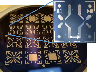
A completed circular semiconductor wafer showing a grid of sixteen patterned dies.

A fabricated wafer provides a documentary view of repeated process fields across a semiconductor substrate.

The image shows a processed wafer for context; it does not identify a specific AI accelerator, foundry node, yield level, or deposition recipe.The NIST item carries no copyright mark; NIST site terms permit copying and distribution and request agency credit.Credit: NIST.Original sourceNIST public information

Physical and chemical vapor processes, atomic-scale cycles, oxidation, and epitaxial growth create films with different properties and coverage. Engineers choose methods according to material, feature geometry, thermal budget, uniformity, interface quality, stress, contamination, and the needs of later operations.

The chamber is only part of the process. Precursor delivery, vacuum, temperature control, wafer condition, chamber seasoning, cleaning, endpoint behavior, and maintenance history all affect the deposited layer. Measurements must distinguish random variation from systematic drift before the next expensive sequence locks the defect beneath additional material.

Three integration zones on one wafer
FEOL
The active-device region where wells, isolation, channels, gates, sources, and drains are formed.
MOL
Contacts and local structures that connect transistor terminals to the first interconnect levels.
BEOL
The layered metal, via, and dielectric network that distributes signals, clocks, power, and ground.
Integration
The ordered compatibility of modules; a locally good film can still damage an earlier or later structure.
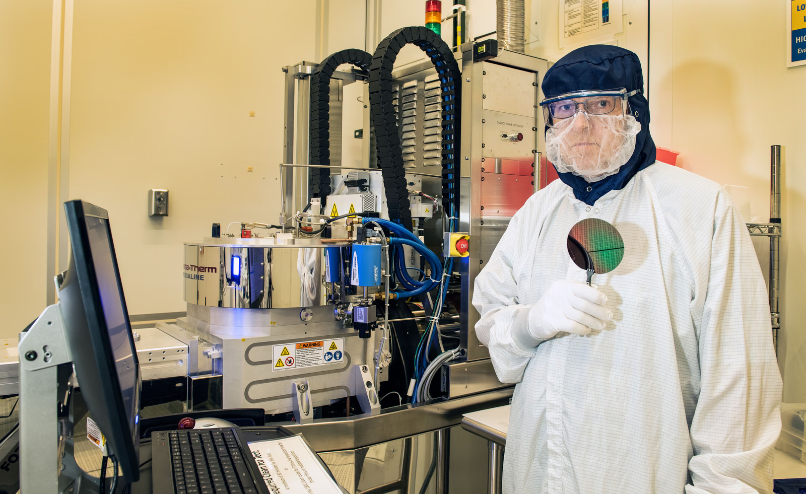
A cleanroom researcher holds a patterned wafer beside a plasma-enhanced chemical vapor deposition tool.

A researcher presents a patterned wafer beside a PECVD tool in a NIST cleanroom.

The scene documents one research process environment; it does not establish commercial-fab throughput, process node, or yield.The unmarked NIST image is public information with agency credit retained. It depicts research PECVD work, not a commercial high-volume fab, process node, or yield result.Curt Suplee / NIST.Original sourceNIST public information

Selective change

Etch removes; implantation changes

The pattern becomes functional only when selected regions acquire the intended geometry and electrical behavior.

Dry and wet etch processes remove chosen materials while preserving others. Their useful result depends on selectivity, directionality, profile, residue, surface damage, and uniformity. Ion implantation introduces dopants with controlled species, energy, and dose; subsequent thermal processes activate or redistribute them within a constrained thermal budget.

Intel describes leading-edge wafers as passing through thousands of process steps over weeks. Exact routes vary, but the complexity means each operation inherits the surface created before it and prepares the interface for what follows. Local optimization can reduce total yield if it damages a downstream margin.Claim

Process language
Selectivity
Preference for removing one material over another.
Profile
The shape and angle left after material removal.
Dose
The amount of implanted species delivered.
Thermal budget
Cumulative heating compatible with existing structures.
Pattern transfer is a coupled loop
  1. Prepare— Condition and verify the incoming surface, chamber state, and material delivery path.
  2. Form— Deposit or grow a film with target composition, thickness, stress, and conformity.
  3. Pattern— Define protected and exposed regions with a controlled imaging and resist process.
  4. Transfer— Etch selectively while controlling profile, damage, residue, loading, and endpoint.
  5. Reset— Strip, clean, inspect, and decide whether the wafer can proceed, rework, or must stop.

Spread 10 / Planarization and clean

Surface control

Each layer needs a usable horizon

Topography accumulates as films are added and patterned; planarization restores a surface the next lithography step can manage.

Chemical-mechanical planarization combines surface chemistry, slurry particles, pad behavior, pressure, motion, and endpoint control to remove material selectively and flatten the wafer. The process must balance removal rate, within-wafer uniformity, selectivity, scratching, dishing, erosion, residue, and compatibility with surrounding structures.

Consumables become part of tool performance. Slurry age and distribution, pad conditioning, carrier condition, retaining rings, filters, and post-polish cleaning can all influence results. Engineers monitor not only the mean thickness but spatial patterns that can reveal equipment wear, process loading, or upstream variation.

Why AI cares: Advanced logic and memory depend on many aligned layers. Lost planarity can narrow focus, distort later patterns, and reduce the yield of large, valuable dies.
Planarity must be judged at several scales
ScaleFailure modeDownstream consequence
FeatureDishing, erosion, recess, or residueResistance, contact, or pattern-transfer error
DiePattern-density-dependent removalFocus and film-thickness variation
WaferNonuniform pressure, slurry, pad, or temperatureEdge loss and systematic yield signature
Tool fleetPad aging, conditioner drift, or chamber mismatchLot-to-lot shift and hidden capacity loss

Reset

Clean without erasing the device

A successful clean removes particles, films, metals, or residues while preserving fragile intended surfaces.

Cleaning methods use liquids, gases, plasma, heat, and mechanical energy in carefully controlled sequences. The target changes throughout the route: photoresist, etch residue, metallic contamination, native oxide, slurry particles, or organic films. A chemistry effective on one surface may corrode, roughen, charge, or alter another.

The thousands-step character of leading-edge wafer processing makes cleaning a repeated integration task, not housekeeping. Rinse quality, drying, queue time, atmospheric exposure, carrier cleanliness, and tool-to-tool transport can affect the next interface. Process windows must account for the state in which a wafer actually arrives.Claim

Surface handoff
  1. Identify— Define the contaminant and vulnerable materials.
  2. Remove— Apply a selective clean with controlled energy.
  3. Rinse— Displace chemistry without redeposition.
  4. Dry— Avoid marks, collapse, corrosion, or particles.
  5. Protect— Control queue time and environment before the next tool.
A clean step needs an endpoint and a damage budget
  1. Name— Specify particles, metals, organics, native film, slurry, polymer, or mobile ions to remove.
  2. Select— Choose chemistry, energy, time, and mechanics compatible with exposed materials and features.
  3. Rinse— Prevent redeposition, watermarking, cross-contamination, and chemical carryover.
  4. Dry— Control stiction, residue, charging, and surface change before the next module.
  5. Verify— Measure both removal effectiveness and unintended loss, roughness, corrosion, or electrical damage.

Spread 11 / Metrology and inspection

Observation

You cannot control what you cannot see

Metrology measures process characteristics; inspection searches for defects and abnormal signatures across wafers and lots.

Critical dimensions, overlay, film thickness, composition, surface shape, electrical behavior, and defectivity require different measurement techniques. Some methods sample selected sites; others scan broad areas. Some are non-destructive and in-line; others require dedicated structures, preparation, or destructive analysis.

The measurement plan balances sensitivity, speed, sampling, cost, and actionability. A highly sensitive tool that reports too slowly may be suited to engineering analysis but not rapid lot disposition. A fast monitor may detect drift without identifying root cause. Strong control strategies connect complementary measurements rather than expecting one instrument to answer every question.

Metrology
Measurement of dimensions, films, properties, or alignment.
Inspection
Detection and classification of defects or abnormal patterns.
Sampling
Which wafers, fields, sites, or features are measured.
Control limit
A statistical signal that triggers investigation or action.
Measurement-system terms
Accuracy
Closeness to an accepted reference under a defined method and uncertainty.
Precision
Closeness among repeated results; precise readings can still share a bias.
Repeatability
Variation under the same instrument, method, operator, and short-term conditions.
Reproducibility
Variation when instruments, sites, operators, methods, or time conditions change.
Sampling risk
Probability that measured sites miss a spatial, temporal, or rare defect population.

Feedback

A measurement matters when it changes action

The control loop turns observations into containment, correction, and verified recovery.

KLA's manufacturing overview frames inspection, metrology, and data analysis as a feedback loop used to detect defects and control semiconductor yield. Measurements become operational when they are tied to wafer genealogy, tool state, recipe, maintenance, material lot, and downstream electrical results.Claim

Engineers distinguish common variation from special causes, look for spatial and temporal signatures, and test potential mechanisms. Automatic process control may adjust settings within defined bounds, while larger excursions require holds and review. Closing the loop means proving that the corrective action removed the signal without creating a new failure elsewhere.

Learning loop
  1. Measure— Capture a trustworthy signal and context.
  2. Associate— Link the signal to process and wafer history.
  3. Diagnose— Test causes against spatial, temporal, and physical evidence.
  4. Correct— Change equipment, recipe, material, or procedure.
  5. Confirm— Verify recovery in process and electrical results.
Close the measurement-to-action loop
  • Define which process decision the measurement can authorize, adjust, hold, or stop.
  • Verify calibration, reference traceability, uncertainty, matching, recipe version, and environmental sensitivity.
  • Choose sites and frequency from defect physics and excursion speed, not only from inspection cost.
  • Retain raw data, wafer coordinates, tool genealogy, and correction history so trends remain reconstructable.
  • Measure false alarms, escapes, response time, and yield impact; more data is not automatically more control.
  • Set guardrails on automated corrections so noise or model drift cannot steer the process unchecked.

Spread 12 / Cleanroom and utilities

Manufacturing environment

The room is part of the tool

Airflow, temperature, humidity, vibration, cleanliness, and human procedures shape what precision equipment can achieve.

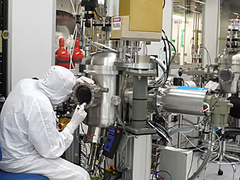
A cleanroom worker inspecting a semiconductor wafer inside process equipment.

A technician works in a semiconductor cleanroom, showing the controlled environment around wafer handling and process equipment.

The image documents cleanroom practice; it does not depict a complete leading-edge production fab or identify an AI-specific wafer process.The NIST item carries no copyright mark; NIST site terms permit copying and distribution and request agency credit.Credit: NIST.Original sourceNIST public information

Cleanrooms use filtered airflow, pressure relationships, material protocols, garments, cleaning, and monitoring to limit particles and molecular contamination. Precision areas may also require stringent temperature, humidity, acoustic, electromagnetic, and vibration control. People and maintenance activities are designed into the contamination plan rather than treated as exceptions.

Automation moves carriers between tools while preserving wafer identity and route. Yet human judgment remains central: technicians maintain equipment, process engineers interpret signals, facilities teams stabilize utilities, and operators coordinate holds and recoveries. The factory's precision is an organizational property as much as a mechanical one.

Contamination travels through more than room air
PathControlEvidence
AirborneFiltration, airflow, pressure, garments, and activity controlParticles by location, size, and operating state
MolecularMaterial selection, exhaust, chemical segregation, and monitoringSpecies-specific surface or air result
ContactCarrier, robot, tool, glove, and maintenance disciplineGenealogy and surface inspection
UtilityUPW, gas, vacuum, drain, and point-of-use purityTrend across supply and return boundaries

Facilities system

Production tools rest on support tools

Power, gases, vacuum, chemicals, water, cooling, exhaust, abatement, and controls must stay within specification together.

Intel's representative advanced-fab description includes about twelve hundred production tools and fifteen hundred utility-support tools. The figures are vendor-provided and facility-specific, but they expose the hidden plant beneath wafer processing: pumps, filters, chillers, treatment systems, delivery skids, sensors, and controls.Claim

A utility excursion can affect many chambers at once, producing common-mode risk that individual tool redundancy cannot solve. Facilities engineering therefore tracks capacity, quality, transient behavior, maintenance isolation, backup states, alarm response, and recovery qualification. Adding a process tool may require upstream utility and downstream abatement changes before installation creates usable capacity.

Capacity test: A production tool is not truly installed until facilities, automation, process recipes, measurement, staffing, maintenance, and yield control are ready with it.
Qualify the room as part of the process
  1. Define— Set environmental and utility limits by zone, tool state, process sensitivity, and recovery need.
  2. Baseline— Measure empty, idle, and operating conditions before production attribution begins.
  3. Challenge— Test power, airflow, alarms, isolation, exhaust, and recovery during credible disturbances.
  4. Correlate— Connect room and utility signals to tool, wafer, maintenance, and defect genealogy.
  5. Control— Use excursion rules that identify affected work, restore state, and verify root-cause closure.
04

Yield, factory learning, and handoff

Productive capacity is saleable output at qualified performance—not floor space, tool count, wafer starts, or a process-node label alone.

Spread 13 / Cycle time and yield learning

Factory flow

A wafer route is a queueing system

Cycle time depends on processing, transport, holds, batching, rework, qualification, and the changing bottleneck across the route.

Intel describes leading-edge wafer manufacture as thousands of process steps over weeks. The exact route varies, but the long loop means work in progress accumulates value and information slowly. A late defect can strand many subsequent operations; a long feedback delay allows the same excursion to affect more lots.Claim

Factory control manages dispatching, batch formation, recipe qualification, preventive maintenance, engineering lots, rework, and priority. Optimizing one tool's utilization can worsen total flow if it creates queues, starves a downstream step, or delays learning. Productive cadence is a property of the route, not the peak speed of its most visible machine.

Cycle-time losses
  • Waiting for the next qualified tool or batch
  • Measurement and engineering disposition holds
  • Maintenance, setup, and recipe qualification
  • Rework or additional inspection after abnormal signals
  • Transport and scheduling across a re-entrant route
Fab flow metrics answer different questions
Raw process time
Time required if a wafer never waits for a tool, batch, hold, or decision.
Cycle time
Elapsed release-to-completion time, including queues, holds, rework, and transport.
WIP
Work released but not complete; location and age matter more than one aggregate count.
Throughput
Conforming output over a stated period, product mix, and process boundary.
Yield
Accepted output divided by an explicit starting population and acceptance rule.

Learning

Yield is knowledge made repeatable

Nominal wafer capacity becomes valuable only when enough dies meet function, performance, power, and reliability requirements.

Yield loss can arise from random defects, systematic pattern issues, process variation, design sensitivity, equipment excursions, assembly interactions, or test limits. Large dies expose more area to potential defects, while aggressive performance bins can reduce the share that meets a particular product target. One headline yield number hides those mechanisms.

Inspection, metrology, and analysis create the process-control loop that improves yield. Teams segment results by layer, structure, tool, time, layout region, and electrical signature, then feed learning into recipes, maintenance, design rules, and future revisions. The same learning can be product-specific, so a qualified process is not automatically a mature product.Claim

Output measures
Wafer starts
Wafers entering a process; not completed output.
Defect density
A measure of defect occurrence over area.
Die yield
The share of fabricated dies meeting a defined screen.
Bin
A performance or quality category assigned during test.
Yield improvement can trade against flow
InterventionPotential benefitWatch metric
More inspectionEarlier containment and richer defect learningQueue time, false alarms, and sampling escape
Tighter holdsPrevents suspect work from advancingHold age, disposition latency, and WIP growth
ReworkRecovers selected wafersAdded cycle time, damage risk, and final reliability
Recipe splitTests a corrective hypothesisComparability, lot genealogy, and capacity fragmentation
Faster releaseReduces waiting after reviewEvidence completeness and repeat excursions

Spread 14 / Fab construction and workforce

Capital project

A fab is built, installed, qualified, and learned

Construction completion is only one milestone on the path to stable, saleable semiconductor output.

Intel characterizes a representative modern fab as an investment of roughly ten billion dollars that can take three to five years to build. It is a vendor example, not a universal cost curve, but it shows why schedule language needs precision: shell, utilities, tool move-in, process qualification, customer qualification, yield ramp, and volume production are different states.Claim

Long-lead tools and utility systems must be ordered against an expected process and product mix. Delays can shift demand, equipment generations, incentives, or customer plans before output arrives. Phased construction can preserve optionality, but only if site utilities, clean space, staffing, and tool connections can expand without destabilizing operating lines.

Status discipline: Announced investment, building area, installed tools, qualified wafer capacity, and saleable product output are not interchangeable measures.
Capital becomes capacity through staged evidence
StateWhat can be claimedWhat cannot yet be claimed
AnnouncedSponsor intent and stated scopeFinancing, construction, or output
AwardedGovernment obligation subject to termsFull disbursement or matching private spend
Under constructionPhysical work has begunTool-ready or production-ready facility
Installed/acceptedEquipment is in place and passes acceptanceProduct-qualified volume
Qualified/HVMNamed products meet release criteria at sustained operationUniversal fungibility across nodes or products

Workforce

The process lives in people and routines

Factories accumulate tacit knowledge about equipment behavior, process interactions, recovery, and the interpretation of weak signals.

A representative advanced fab's thousands of production and utility-support tools require operators, process and equipment engineers, technicians, facilities specialists, automation teams, contamination control, quality, safety, suppliers, and construction trades. The exact staffing model varies, but no equipment purchase substitutes for this operating system.Claim

Workforce ramp has several clocks. Classroom learning covers principles and procedures; supervised practice builds safe execution; repeated excursions build diagnostic judgment; cross-team routines make recovery fast. Supplier field service and local training pipelines are part of capacity. A site may own identical equipment yet ramp differently because its experience, maintenance discipline, and feedback culture differ.

Capability layers
  • Safe, repeatable tool operation and material handling
  • Preventive maintenance and calibrated recovery
  • Process integration across many interacting modules
  • Facilities stability and common-mode risk management
  • Fast learning from inspection, test, and customer evidence

Selected final CHIPS direct-award ceilings

NIST's final-award records list these maximum direct funding amounts. They are award ceilings—not company capital expenditure, cash disbursed to date, installed wafer capacity, production output, or comparable project scope. Map logic, memory, analog, power, and packaging capability separately because nominal wafer capacity is not automatically substitutable.
Final direct awardUSD billions
View chart values
Selected final CHIPS direct-award ceilings — underlying values in USD billions
CategoryFinal direct award
Intel$7.87B USD billions
Samsung$4.75B USD billions
Micron$6.17B USD billions

Data status: final direct-award ceilings. Compare project geography, technology, milestones, private spend, and operating dates separately.

Spread 15 / Known-good die and handoff

Test and disposition

A patterned wafer is not yet a usable accelerator

Wafer-level electrical tests classify dies, inform yield learning, and guide which pieces should receive scarce packaging capacity.

Test structures and product probes measure whether fabricated circuits behave within defined limits. Results support process control, failure analysis, performance binning, and die disposition. Screening must balance test coverage, time, contact quality, stress, and the fact that some package-level or long-duration failures cannot be observed on the wafer.

The semiconductor value chain moves from front-end fabrication into back-end assembly, test, and packaging. That boundary transfers more than diced silicon: die maps, bin data, handling requirements, traceability, interface specifications, mechanical limits, and known risks must travel with each lot.Claim

Fab exit
  1. Probe— Measure electrical behavior at wafer level.
  2. Map— Record die identity, location, and disposition.
  3. Dice— Separate dies while controlling damage and contamination.
  4. Select— Route known-good candidates to the intended package flow.
  5. Transfer— Preserve data and physical identity into assembly.
Known-good die is a sequence of dispositions
  1. Sort— Test structures and die on wafer while preserving location, test conditions, and binning evidence.
  2. Assemble— Join selected die, substrate, memory, and thermal structures under controlled genealogy.
  3. Final test— Exercise packaged electrical, interface, power, and functional behavior across release conditions.
  4. Bring up— Validate clocks, reset, memory, links, firmware, diagnostics, and platform interaction at operating speed.
  5. Qualify— Close reliability, manufacturing, software, and traceability requirements before volume release.

Transition · Package

The next constraint is proximity

Known-good logic becomes an AI engine only when memory, interconnect, power, and thermal paths can sit close enough around it.

TSMC describes CoWoS as integrating logic chiplets and high-bandwidth memory on an interposer in an advanced package. The statement is a vendor description of its platform, but it captures the architectural handoff: packaging now determines how much compute and memory can communicate within a compact power and thermal envelope.Claim

That handoff crosses a globally specialized chain. Fab yield determines the supply of candidate die; packaging capacity determines how many can be assembled; memory supply and package yield determine complete output. Precision therefore continues beyond the cleanroom in substrates, interposers, bonding, test, cooling interfaces, and final system qualification.Claim

Continue: Volume III · Package follows logic die, high-bandwidth memory, substrates, interposers, bonds, thermal limits, and final test into one integrated device.
Post-silicon evidence must return to its owner
ObservationPrimary feedback pathDisposition question
Systematic electrical failDesign, PDK model, process integration, or testFix in silicon, screen, or specification?
Package-linked failAssembly, substrate, interconnect, or thermal designRework, process change, or redesign?
Marginal performanceTiming, power, cooling, firmware, or binningGuardband, optimize, down-bin, or reject?
Intermittent field behaviorReliability, platform, telemetry, and failure analysisContain population and preserve evidence?
Installed fab capacity becomes AI capacity only after packaging, memory, systems, networks, power, and software complete the chain.

Behind the claim

Evidence, in context.

Opening the evidence record…